

At present, with the promotion of localization, the demand for mask plates by semiconductor companies is constantly increasing; At the same time, semiconductor materials are at the upstream link of the entire industry chain, which will also play an important role in the development of the semiconductor industry
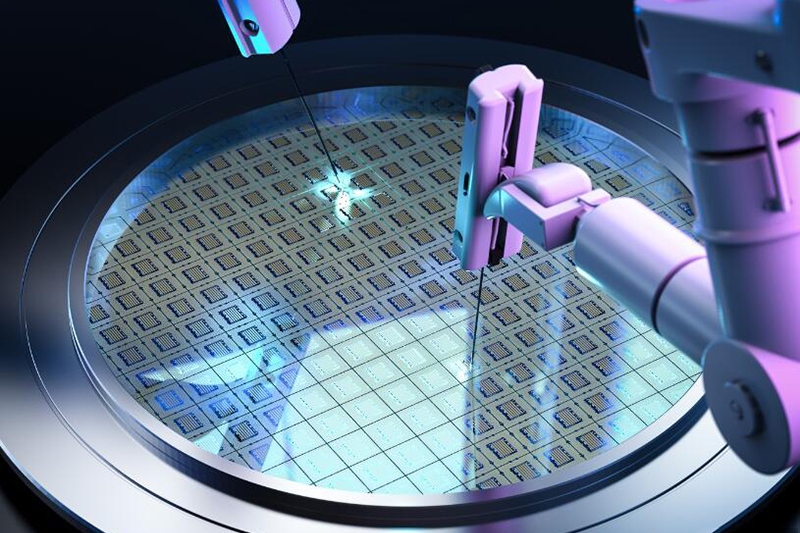
Nowadays, photolithography technology is a key technology necessary for manufacturing chips, and the photomask plate in photolithography technology is a very important part.
The demand for mask plates is growing rapidly, and the gap in domestic production level is still significant
With the continuous expansion of overall demand in the semiconductor industry, the global scale of photomask plates is also gradually increasing: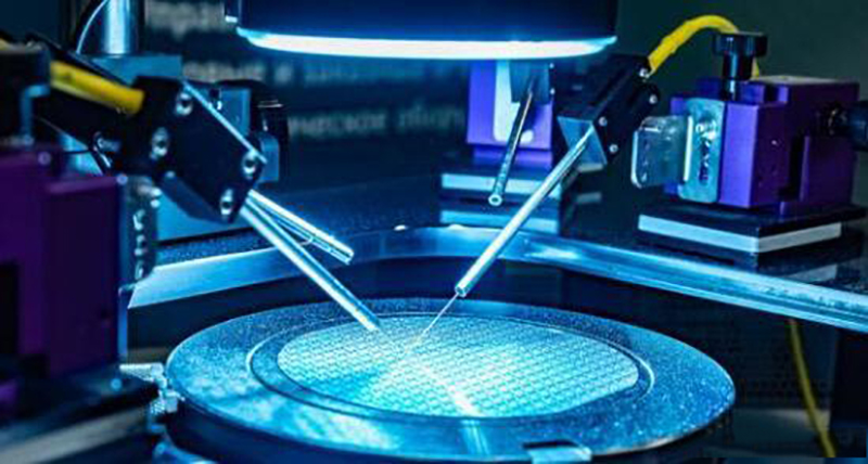
According to SEMI's market forecast for the global mask plate industry, the market size of the global mask plate industry will grow at a compound annual growth rate of about 16% from 2023 to 2028; It is expected that by 2028, the market size of the global mask plate industry will reach approximately 62.3 billion yuan.
In the semiconductor field, photomask manufacturers can be divided into two categories: wafer fabs/IDM factories with their own supporting factories and independent third-party photomask manufacturers, including Intel, Samsung, TSMC, SMIC, etc., all of which have their own mask plate businesses.
Among them, among the market share of various manufacturers, the proportion of wafer/IDM factories has steadily increased, accounting for only 39% in 2008, 64% in 2018, and 65% in 2019. Independent third-party mask manufacturers account for 35%.
From a global perspective, mask manufacturers are mainly concentrated in Japan and the United States, including Japanese Toppan (relief printing), Japanese DNP (Greater Japan Printing), American Photonics (Phoenix), Japanese HOYA (Hoya), Korean LG-IT (LGInnotek, a subsidiary of LG Group), and other manufacturers.
Looking back at China, there is still a significant gap between Chinese mask plates and foreign mask plate manufacturers due to the following issues:
1. Technical bottleneck: Compared to the international leading level, there is still a significant gap in the manufacturing technology of photomask plates in China, which cannot meet the application needs of high precision and high reliability.
2. Equipment update: Compared to the international leading level, the update and replacement speed of China's photomask plate production equipment is slower, which also restricts the improvement of its technical level.
3. Intellectual Property: There are problems with the protection of intellectual property rights in Chinese photomask plates. Some technologies and products are stolen or infringed upon, which directly affects the interests and innovation enthusiasm of enterprises.
In a sense, with the continuous development of China's semiconductor industry and increased government support for the industry, the Chinese photomask plate industry is gradually improving its technological level and market competitiveness.
Semiconductor mask: an indispensable tool for pattern transfer in photolithography
Masks, as an important tool for graphic transfer, transfer the carried circuit graphics to substrate materials such as silicon wafers through exposure, and are widely used in fields such as semiconductors, flat panel displays, circuit boards, and touch screens. Taking TFT-LCD manufacturing as an example, by utilizing the exposure masking effect of the mask plate, the designed TFT array and color filter pattern are sequentially exposed and transferred to a glass substrate in the order of the film layer structure of the thin film transistor, ultimately forming a display device with multiple film layers superimposed; Taking wafer manufacturing as an example, the manufacturing process requires multiple exposure processes, utilizing the exposure masking effect of the mask to form gates, source drain electrodes, doping windows, electrode contact holes, etc. on the surface of the semiconductor wafer. Compared to other important parameters such as minimum linewidth, CD accuracy, and positional accuracy, semiconductor masks are significantly higher than mask products in fields such as flat panel displays and PCBs.
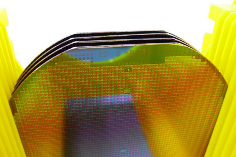
Upstream substrate: Mask substrate, shading layer, protective film
Mask plates are usually composed of a substrate, a shading layer, and a protective film. The substrate is mainly made of glass (quartz or soda). Due to the advantages of high pass through rate, high flatness, and low coefficient of expansion of quartz, high-purity quartz glass is usually used as the substrate. The manufacturing method of quartz substrates requires the synthesis of quartz substrates through cold processing of quartz ingots. The main supplier in the market is Shinetsu Chemical from Japan; The shading layer is divided into a hard shading layer and a latex shading layer. Latex is mainly used in PCB, touch and other scenarios. In the hard shading layer, due to the high mechanical strength and durability of the chrome plate, as well as the ability to form fine patterns, the current mainstream mask plate usually plated chromium on the substrate to form a shading layer; The protective film is usually a transparent film on an aluminum alloy frame, which plays a protective role on the mask. It has low value but high technical difficulty.
Mid stage manufacturing: photolithography, testing, etc. are all core processes
In the production process of mask templates, the mask processing technology is divided into core key steps such as CAD graphic design, chrome plating, gluing, lithography, development, etching, demolding, cleaning, optical film application, key parameter measurement, detection, and repair.
1) Gluing and lithography are the core processes in manufacturing, which require first coating the mask substrate with adhesive (usually positive photoresist), and then exposing the surface through a lithography machine, usually with 130nm as the boundary. Lithography equipment above 130nm uses laser direct writing equipment. However, as the line width and line distance of the mask plate decrease, serious diffraction phenomena will occur during the exposure process, resulting in lower edge resolution and distortion of the exposed pattern, Therefore, electron beam lithography is usually required for 130nm and below;
2) The measurement and detection of key parameters are crucial to the quality and yield of the mask plate. Key parameters such as critical dimension (CD) and overlay accuracy of the mask plate need to be measured, and automatic optical inspection equipment (AOI) needs to be used Detecting defects generated during the mask manufacturing process and repairing defects and particles during the mask production process through laser and other means;
Downstream classification: Large shipment volume above 130nm, high unit price for 55/65-28nm
Mask plates are generally classified according to the manufacturing process, and the higher the manufacturing process, the more expensive the unit price. According to Semis statistics, the global shipment of photomask plates in 2019 reached 559000 sheets, of which 88000 sheets were shipped for masks below 22nm, accounting for 16% of the global shipment. The shipment of 28-90nm mask plates reached 175000 sheets, accounting for 31%. The shipment of 130nm and above mask plates reached 296000 sheets, accounting for 53%. In the future, with the expansion of 28nm and below processes, this proportion is expected to increase significantly; At the same time, in terms of unit price, there is a significant difference in prices among different processes, with the unit price of 55/65-28nm mask plates ranging from tens of thousands of yuan, while the unit price of 130nm and above is only a few thousand yuan.
The import of mask plates is limited, and there is an urgent need for domestic substitution
The United States has included mask plates below 250nm process nodes in the restriction list. On October 7, 2022, the US Department of Commerce announced the revised Export Management Regulations, increasing export and supply restrictions on semiconductor equipment and components, and upgrading sanctions on China's semiconductor industry. This sanction includes supply restrictions on mask plates, which means that China's import of advanced foreign process mask plates will be hindered. The demand for imported mask plates, which is forced to be compressed domestically, will be filled by domestic mask plates. The process of domestic substitution in the mask plate industry is expected to accelerate.
Domestic wafer factories have crossed the 250nm process, and there is strong certainty of domestic substitution. Domestic wafer fabs have achieved breakthroughs in the 250nm process node. In 2021, the sales of CR3 in domestic wafer fabs accounted for 64% of the total sales, with processes of 130nm and below. In the face of import restrictions, domestic wafer fabs will actively seek domestic alternatives, resulting in strong demand certainty.At present, most top domestic wafer manufacturers need to purchase mask plates externally. After the United States restricts the export of mask plates, there is an urgent need for domestic mask plates to replace them. At present, only SMIC, Huahong Group, and Crystal Integrated have equipped mask plate manufacturing facilities for domestic wafer foundries CR3. Other wafer foundries need to purchase mask plates from third-party manufacturers. In the United States, the export of process masks with a diameter of 250nm and below is restricted, while domestic mask manufacturers have already surpassed the 250nm node in their process, and there is an urgent need to purchase domestically produced mask plates to fill the gap in imported mask plates.
The global market size of semiconductor mask plates is about 5.4 billion US dollars, and the localization rate is expected to rapidly increase. According to Semi statistics, the 2021 mask version accounts for 12% of wafer manufacturing materials, which is the second largest consumable after silicon chips. It is estimated that the global semiconductor mask version market size will be about 5.4 billion dollars in 2022, and the mask version market size in Chinese Mainland will be about 9 billion yuan. At present, manufacturers in Chinese Mainland mainly focus on mask production at 350~180nm process nodes. Some manufacturers have mastered the production technology of 130nm process nodes, and the localization rate of mask versions at 90nm and below will be almost zero. Therefore, with the accelerated expansion of Chinese Mainland wafer factories and the consideration of supply chain security, the localization rate of high-end masks in the future is expected to increase rapidly.
Benefiting from the transfer of flat panel display capacity to Chinese Mainland, the panel mask is also expected to accelerate domestic substitution. According to the statistics of CINNO Research, the manufacturing capacity of LCD/OLED in Chinese Mainland will account for 72%/40% of the world respectively in 2022, and the global flat panel display manufacturing capacity will accelerate its transfer to Chinese Mainland. In 2022, the global flat panel display mask market will be about 5 billion yuan, and the market in Chinese Mainland will be about 3 billion yuan. According to our estimates, the market share of domestic panel mask suppliers in 2022 will be only 20% in total. We believe that with the transfer of the panel industry chain to Chinese Mainland and the increase of OLED penetration, the localization rate of panel mask is also expected to accelerate.

