

Although the overall prosperity of the semiconductor industry is poor, there is a type of key materials that are in short supply.
According to ET News in South Korea, the supply of semiconductor photomasks is in short supply, with several major photomask suppliers holding high orders, including Photonics, Toppan, DNP, etc.
Under normal circumstances, the shipping time for high specification photomask products used to be 7 days, but now it has been extended to 30-50 days, which is 4-7 times longer than the original time; The delivery time of low specification products has also doubled compared to previous days.
Industry concerns suggest that the price of this material may increase by another 10% -25% from this year's high next year, and delivery times may be further extended.
At present, the semiconductor industry is facing a cold winter, but the price of photomasks is rising against the trend, which is quite rare. In fact, the gap between supply and demand mainly comes from two aspects:
Firstly, semiconductor manufacturers have revealed that delayed delivery of equipment such as photomask electron beam etching has hindered photomask production.
Secondly, it comes from the demand side. It is understood that the soaring demand mainly comes from system level chips, especially high-performance chips such as automotive chips and autonomous driving chips. The strong demand in downstream fields is driving IC design factories to expand their orders, thereby intensifying the demand for photomasks.
In this situation, industry insiders predict that semiconductor contract manufacturers may further delay their production schedules, and contract manufacturing prices will rise accordingly; The problem of car chip shortage, which has gradually begun to ease recently, may shift back to shortage.
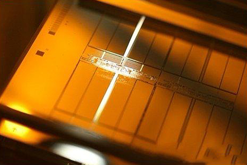
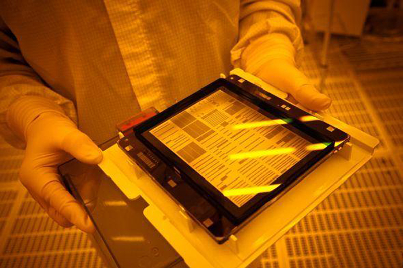
Public information shows that in the semiconductor manufacturing process, photolithography technology is required to form patterns on chips. In order to copy the graphics onto the wafer, the help of a photomask is necessary - this process is similar to using a negative to copy the image onto the photo when developing a photo, so photomask is also known as the "negative" of lithography technology.
The upstream of the photomask plate industry chain are suppliers of components such as mask substrates, optical films, chemical reagents, etc; Midstream is a manufacturer of photomask plates from Japan, including HOYA, DNP, LG-IT, SKE, SMIC, and Qingyi Optoelectronics; Downstream applications include semiconductors, LED chips, display panels, touch panels, and other fields.
From an upstream perspective, mask substrates can be divided into resin substrates and glass substrates based on different materials. Among them, glass substrates include quartz glass, soda glass, borosilicate glass substrates, etc. Quartz glass substrates have the characteristics of good wear resistance, low thermal expansion rate, high optical transmittance, and long service life, and are currently the mainstream products for mask substrates.
From the midstream perspective, the global photomask plate market is currently dominated by Japanese, Korean, and American companies, with only local companies such as SMIC and other foundries producing their own semiconductor mask plates and Qingyi Optoelectronics having advantages in the field of flat panel display masks. At present, domestic photomask products are mainly concentrated in the mid to low-end market, and the degree of localization in the market is relatively low. In the high-end market, domestic photomask products are still blank. In the future, domestic enterprises need to continuously increase their technological research and development efforts and product innovation efforts, in order to accelerate the process of domestic substitution.
Mask market size
The global market size of photomasks is increasing year by year. According to data released by SEMI, the global semiconductor chip mask market reached 3.7 billion US dollars in 2017, a year-on-year increase of 13%; In 2019, the global market size was approximately 4.3 billion US dollars.
In terms of domestic demand, in 2019, the Chinese semiconductor photomask market reached 144 million US dollars. From the specific demand for glass substrates, the demand for IC photomask glass substrates increased from 29000 square meters in 2015 to 56000 square meters in 2020, surpassing the demand for FPD (flat panel display) photomask glass substrates for the first time.
According to data, the scale of China's integrated circuit market will reach 1139.7 billion yuan in 2022; The market size of semiconductor mask plates in China was approximately 5.3 billion yuan in 2020, and it is expected to reach 9.4 billion yuan by 2025.
Masking competition pattern
In the semiconductor field, photomask manufacturers can be divided into two categories: wafer fabs/IDM factories with their own supporting factories and independent third-party photomask manufacturers, including Intel, Samsung, TSMC, SMIC, and China Resources Microelectronics (DSM), all of which have their own mask business. Due to the fact that the mask plate involves confidential technology from Foundry, most of the mask plates used in Foundry's advanced processes (below 45nm) are produced by their own professional factories. However, for mask plates used in more mature processes such as 45nm and above, Foundry tends to purchase from independent third-party mask plate manufacturers in order to reduce costs.
In the market share of various manufacturers, the proportion of wafer/IDM factories has steadily increased, accounting for only 39% in 2008, 64% in 2018, and 65% in 2019. Independent third-party mask manufacturers account for 35%.
The world's independent third-party mask manufacturers are mainly concentrated in Japan and the United States, including Toppan (relief printing), DNP (Japanese printing), Photonics (Phoenix), HOYA (Japan), SKE (SK Electronics), LG-IT (LGInnotek, a subsidiary of LG Group), etc., as well as Chinese manufacturers such as Taiwan, China masks, Luwei Optoelectronics and Qingyi Optoelectronics.
Pain points in the development of domestic mask plates
1. As mask plates are an important link between design and manufacturing, wafer manufacturers have their own professional factories to produce the mask plates they need. International giants like Intel and Samsung have tightly grasped the mask manufacturing process and established their own mask factories. Therefore, advanced mask plate technology is also in the hands of wafer factories with advanced wafer manufacturing processes
2. The characteristics of high investment, small scale, high technological precision, and zero product defects in semiconductor mask plates have deterred many companies that are concerned about no returns. There are few large-scale and market-oriented mask plate enterprises in China. There are several large-scale domestic companies specializing in the production of mask plates, including Luwei Optoelectronics, Qingyi Optoelectronics, and SMIC. However, Luwei Optoelectronics and Qingyi Optoelectronics mainly produce mask plates for display screens.
3. 2 major technical difficulties: Firstly, the transparency of the material, which requires the light mask to be 100% opaque and the substrate to be 100% transparent; The second one is purification technology, which requires quartz to be purified to electronic grade (minimum purity requirement of 99.9999%). Due to the immaturity of technology in our country before, we could only transport quartz to foreign countries, undergo a series of difficult processes such as grinding, refining, and purification, process it into quartz ingots, and then repurchase them at a high price. There is a huge difference in price between this one in and one out. The export price of quartz is $400 per ton, and the import price of quartz ingots is $10000 per ton.

