Two photon lithography: breaking through the packaging bottleneck of optoelectronic chips
As a rising star in the semiconductor industry, optoelectronic chips have important application prospects in fields such as optical interconnection, optical computing, optical sensing, and LiDAR, and have become a focus of attention from all walks of life, opening up a new track for the development of the post Moore's Law era. Thanks to the mature semiconductor CMOS process, the preparation capability of optoelectronic chips has been rapidly developed.
However, there are still key technological bottlenecks in the packaging process of optoelectronic chips. The packaging process of optoelectronic chips, in addition to the well-known interconnection of electrical signals, also needs to consider the coupling of optical signals between different modules, which requires solving the optical interconnection problem between fiber chips and chip chips. There are two main challenges:
1. Optical chips involve multiple material systems and structures, and there are significant differences in the size and distribution of different beam modes. Cleverly solving the problem of mode field mismatch during packaging can achieve efficient coupling between multiple material systems and structures.
2. The beam size in the waveguide on the chip is in the micrometer range, requiring high-precision alignment to achieve efficient coupling, which puts higher demands on the alignment accuracy of the packaging process.
The two-photon lithography technology based on two-photon absorption process, as a three-dimensional printing process in micro and nano sizes, can accurately prepare any three-dimensional structure, which is expected to solve the bottleneck of optoelectronic chip packaging process.
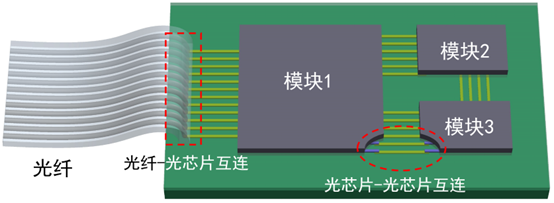
On the one hand, three-dimensional curved surfaces or gradient waveguide structures can be integrated on the chip to shape the beam through reflection or adiabatic compression, achieving ultra wide band mode field transformation;
On the other hand, the morphology of three-dimensional structures has high geometric degrees of freedom, which increases the flexibility of on-chip mode field manipulation, thereby achieving more efficient coupling and interconnection.
In addition, two-photon lithography can also prepare connection structures after sub module assembly, effectively reducing the alignment accuracy requirements during the packaging process.
Therefore, in the packaging of optoelectronic chips, two-photon lithography technology has important application value and has been widely explored. Currently, there are mainly three technical routes.
Optical Packaging Method Based on Two Photon Lithography
1. Photon wire bonding
Drawing inspiration from the widely used lead bonding and photon lead bonding technology in microelectronics, a two-photon lithography process is adopted to directly print polymer waveguides between the waveguides to be connected. By gradually changing the waveguide cross-section, adiabatic transformation of the mode field is completed, thereby achieving efficient interconnection between different waveguides. This method has been validated in optical interconnection and coherent communication, and is suitable for various application scenarios such as fiber chip, chip chip, etc.
2. Micro Freeform Surface
Print miniature optical free form surfaces on the waveguide end face, shape the outgoing light field of the waveguide in the form of reflection or refraction, regulate the mode field distribution and propagation direction, and thus complete the mode field transformation. The adopted structure has low dispersion, which is beneficial for Wavelength insensitive, it has been verified that ultra wideband coupling from visible near-infrared is compatible with wafer level testing and packaging, enabling high-density interconnect packaging.
3. Mechanical alignment guide structure
Two photon lithography technology can also be used to print mechanical alignment guidance structures, assisting in achieving high-precision alignment during the coupling process. Printing an inverted cone structure on the grating coupling region to guide the alignment process of the fiber can achieve sub micron level alignment accuracy without introducing significant additional losses, and is expected to be applied in pluggable devices.
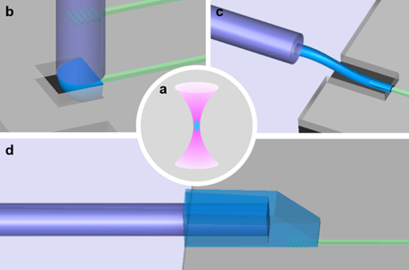
Exploration of commercialization
With the gradual entry of optoelectronic chips into the market, packaging technology based on two-photon lithography has also begun commercial exploration. Large scale commercial applications not only focus on coupling characteristics such as bandwidth and insertion loss, but also need to consider more factors. For example, whether two-photon lithography can stably and reliably prepare high-quality three-dimensional structures, whether it can meet the industry's processing speed and accuracy requirements, and whether it has user-friendly ease of use and maintenance.
Currently, multiple companies have opened up the commercial market for two-photon lithography. NanoScribe, Vanguard, Heidelberg and other companies have launched commercial two-photon lithography equipment, which has made significant progress in scanning speed, processing accuracy, alignment accuracy, etc. Dream Photonics, PHIX and others mainly provide process services and can directly provide packaging services based on two-photon lithography to the outside world. The application of two-photon lithography technology in optoelectronic chip packaging has taken a solid step towards large-scale commercial development.
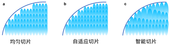
Figure 3: Three slicing methods: uniform slicing, adaptive slicing, and intelligent slicing.
The packaging method based on two-photon lithography technology has made significant progress and has been widely recognized by various sectors after more than a decade of exploration. However, opportunities always coexist with challenges. In the era of explosive growth in communication capacity, whether two-photon lithography technology can occupy an important position in optoelectronic chip packaging depends on whether it can meet the future large-scale application needs. Based on this, the author also outlines the future development trends in this field.
1. Significantly improve preparation efficiency
The current point by point scanning method has a slow preparation speed and is difficult to meet the efficiency requirements of large-scale production. On the one hand, new two-photon exposure methods such as multi beam and layer by layer can be used to improve the preparation speed. On the other hand, other preparation processes can also be explored, such as nanoimprinting, which can upgrade the serial processing method to parallel to meet the wafer level preparation requirements.
Figure 4: Three exposure methods: point by point, layer by layer, and multi beam exposure.
2. Developing multiple types of lithography materials
Two photon lithography mostly acts on photosensitive polymer materials. Compared to conventional semiconductors or dielectric materials, polymer materials have a large coefficient of thermal expansion, limited range of refractive index selection, and poor long-term stability. At the same time, the shrinkage of polymers during the crosslinking process also poses certain challenges to the morphology control of three-dimensional structures. Exploring organic-inorganic hybrid composite photosensitive materials can to some extent solve the above-mentioned problems.
3. Optimizing design modeling methods
The 3D structure has a high degree of geometric freedom, which brings great convenience to wave front control. But the many parameters regulated by the design bring great pressure to the simulation design process. It is necessary to combine geometric optics and wave optics methods for computational exploration and construct a new modeling method. Data driven and physics driven machine learning methods can also play important roles in the design and characterization of three-dimensional micro optical structures.
4. Developing new methods for structural characterization
Micro three-dimensional optical structures, with scales between macroscopic and microscopic, have small structures and large curvatures. Conventional measurement methods such as white light interference, electron microscopy, and atomic force microscopy are difficult to effectively measure, and there is an urgent need for new characterization methods. Based on multi quadrant electron microscopy 3D reconstruction, it is expected to achieve accurate measurement of micro free-form surface morphology. X-ray micro tomography is also a promising characterization method.
Two photon lithography technology can accurately prepare three-dimensional structures and integrate them onto optoelectronic chips. It can construct a large bandwidth and low loss optical signal link between fiber chips and chip chips, achieve efficient interconnection of optical signals, reduce alignment accuracy in the packaging process, and bring new opportunities to the packaging process of optical chips. With the iterative evolution of technology and further development of the industry, we expect that the optoelectronic chip packaging architecture based on two-photon lithography will be widely applied to solve the packaging problems of optoelectronic chips.